
Summary of NEW LOW-POWER, GENERAL-PURPOSE LATTICE FPGA FAMILY
Lattice Semiconductor launched the Certus-NX FPGA family, featuring high I/O density, low power consumption, compact 28 nm FD-SOI packages, and rapid "instant-on" performance. Supporting PCIe and Gigabit Ethernet, these devices enable efficient data processing and system management across industrial and communication sectors.
Parts used in the Lattice Certus-NX FPGA Family:
- Lattice Nexus platform
- 28 nm FD-SOI process technology
- AES-256 encryption module
- ECDSA authentication block
- Programmable back bias circuitry
- SPI memory interface
- 1.5 Gbps differential I/O
- 5 Gbps PCIe IP block
- 1.5 Gbps SGMII IP block
- 1066 Mbps DDR3 IP block
- Certus-NX development boards
Lattice Semiconductor has introduced a new general-purpose FPGA family that has been developed to combine high I/O density, low-power, small packages and fast interfaces.
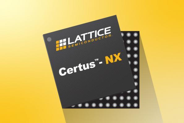
The Lattice Certus-NX series provides up to double the I/O density per mm 2 of similar FPGAs, and provides power savings, a small footprint, reliability, and instant-on performance. Devices in the family support PCI Express (PCIe) and Gigabit Ethernet interfaces to provide faster data co-processing, signal bridging, and system control. General-purpose Certus-NX FPGAs are applicable to a wide range of applications, from data processing in industrial equipment to system management in communications infrastructure. The Certus-NX devices are developed on the Lattice Nexus platform using 28 nm FD-SOI process technology.
Key Features Of The Lattice Certus-NX FPGA Family Include:
- Up to 3x smaller form factor. As an example, Certus-NX FPGAs can provide a full PCIe solution in a 36 mm 2 footprint. Using the smallest package available in the family can still deliver double the I/O density per mm 2 of competing FPGAs for better design flexibility.
- Robust I/O interfacing capability through access to Lattice’s IP library. Notable IP blocks available on Certus-NX include:
- 1.5 Gbps differential I/O with performance that is up to 70 percent higher than competing FPGAs.
- 5 Gbps PCIe, 1.5 Gbps SGMII, and 1066 Mbps DDR3. These IP blocks can be tested on Certus-NX development boards for the fast implementation of interfaces.
- Strong authentication and encryption – Certus-NX FPGAs support AES-256 encryption with ECDSA authentication for the protection of the devices throughout their whole lifecycles.
- Up to 4x lower power consumption – Certus-NX FPGAs feature a programmable back bias to allow user-selectable high-performance or low-power operating modes.
- Instant-on performance – The devices have ultra-fast device configuration from SPI memory that can be up to 12x faster than similar competing FPGAs. Individual I/Os can configure in just 3 ms, and the full-device startup can be achieved in only 8-14 ms depending on device capacity.
Read more: NEW LOW-POWER, GENERAL-PURPOSE LATTICE FPGA FAMILY
- What process technology do Certus-NX devices use?
The devices are developed on the Lattice Nexus platform using 28 nm FD-SOI process technology. - How much faster is the startup time compared to competing FPGAs?
Device configuration from SPI memory can be up to 12x faster than similar competing FPGAs. - Does the Certus-NX family support AES encryption?
Yes, the devices support AES-256 encryption with ECDSA authentication for full lifecycle protection. - Can users adjust power modes on these FPGAs?
Yes, a programmable back bias allows user-selectable high-performance or low-power operating modes. - What is the maximum startup time for the full device?
Full-device startup is achieved in only 8-14 ms depending on device capacity. - Which interfaces are supported by the Certus-NX family?
The family supports PCI Express and Gigabit Ethernet interfaces for faster data co-processing. - How does the I/O density compare to competitors?
The series provides up to double the I/O density per mm² of similar FPGAs. - What form factor reduction does the new family offer?
The family offers an up to 3x smaller form factor, such as delivering a full PCIe solution in a 36 mm² footprint.
