Summary of TI intros its lowest noise octal 12-bit ADC
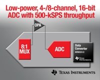
The ADS5294 is an octal-channel, low-power CMOS ADC from Texas Instruments offering up to 80 MSPS sampling at 14-bit resolution. It features high SNR and SFDR, programmable digital processing (FIR decimation, IIR high-pass, digital gain, 2/4-channel averaging), selectable 12/14-bit resolution, and flexible 1- or 2-wire serialized LVDS outputs with programmable input-to-output mapping. Low power (58 mW/ch at 50 MSPS; 77 mW/ch at 80 MSPS) and test patterns ease FPGA capture. Packaged in a 12 mm x 12 mm, 80-pin QFP, it targets high-performance, narrow-band, and cost-sensitive multichannel systems.
Parts used in the ADS5294 Project:
- ADS5294 octal-channel ADC (Texas Instruments)
- 12 mm x 12 mm, 80-pin QFP package
- LVDS interface lines (1- or 2-wire per channel)
- FPGA or LVDS receiver for data capture
- PCB for routing LVDS outputs with programmable mapping
- Power supply capable of supporting ADC power consumption
- Clock source supporting up to 80 MSPS
Description
Using CMOS process technology and innovative circuit techniques, the ADS5294 is a low power 80MSPS 8-Channel ADC. Low power consumption, high SNR, low SFDR, and consistent overload recovery allow users to design high performance systems.
The ADS5294 has a digital processing block that integrates several commonly used digital functions for improving system performance. It includes a digital filter module that has built-in decimation filters (with low-pass, high-pass and band-pass characteristics). The decimation rate is also programmable (by 2, by 4, or by 8). This makes it useful for narrow-band applications, where the filters can be used conveniently to improve SNR and knock-off harmonics, while at the same time reducing the output data rate. The device includes an averaging mode where two channels (or even four channels) can be averaged to improve SNR.
Serial LVDS outputs reduce the number of interface lines and enable the highest system integration. The digital data from each channel ADC can be output over one or two wires of LVDS output lines depending on the ADC sampling rate. This 2-wire interface helps keep the serial data rate low, allowing low cost FPGA based receivers to be used even at high sample rate. The ADC resolution can be programmed to 12 bit or 14 bit through registers. A very unique feature is the programmable mapping module that allows flexible mapping between the input channels and the LVDS output pins. This helps greatly reduce the complexity of LVDS output routing and can potentially result in cheaper system boards by reducing the number of PCB layers.
Features
- Maximum Sample Rate: 80 MSPS/14-Bit
- High Signal-to-Noise Ratio
- 75.5-dBFS SNR at 5 MHz/80 MSPS
- 78.2-dBFS SNR at 5 MHz/80 MSPS and Decimation Filter Enabled
- 84-dBc SFDR at 5 MHz/80 MSPS
- Low Power Consumption
- 58mW/CH at 50 MSPS
- 77 mW/CH at 80 MSPS (2 LVDS Wire Per Channel)
- Digital Processing Block
- Programmable FIR Decimation Filter and Oversampling to Minimize
Harmonic Interference - Programmable IIR High Pass Filter to Minimize DC Offset
- Programmable Digital Gain: 0 dB to 12 dB
- 2- or 4-Channel Averaging
- Programmable FIR Decimation Filter and Oversampling to Minimize
- Flexible Serialized LVDS Outputs:
- One or Two Wires of LVDS Output Lines per Channel Depending on ADC
Sampling Rate - Programmable Mapping Between ADC Input Channels and LVDS Output
Pins-Eases Board Design - Variety of Test Patterns to Verify Data Capture by
FPGA/Receiver
- One or Two Wires of LVDS Output Lines per Channel Depending on ADC
Texas Instruments has introduced a low noise octal-channel, 14-bit analogue-to-digital converter (ADC) and a sampling frequency of up to 80MSPS.
The ADS5294 has specified signal-to-noise ratio (SNR) of 75.5dBFS at 5MHz.
Power consumption is 77mW per channel at 80MSPS.
On-chip TI has included a digital processing block, a low-frequency noise suppression mode and programmable input-to-output mapping.
Using the ADS5294, digital data can be output over one or two wires of LVDS pins per channel reducing the number of interface lines. This creates a two-wire interface which keeps the serial data rate low allowing designers to use low cost FPGAs.
The ADS5294 is available in a 12mm x 12mm, 80-pin QFP package.
For more read: TI intros its lowest noise octal 12-bit ADC
- What is the maximum sample rate of the ADS5294?
The maximum sample rate is 80 MSPS at 14-bit resolution. - What signal-to-noise ratio does the ADS5294 achieve?
It achieves 75.5 dBFS SNR at 5 MHz and 80 MSPS, and 78.2 dBFS with the decimation filter enabled. - How much power does the ADS5294 consume per channel?
Power consumption is 58 mW per channel at 50 MSPS and 77 mW per channel at 80 MSPS (with 2 LVDS wires per channel). - Does the ADS5294 include digital filtering?
Yes, it includes programmable FIR decimation filters (decimation by 2, 4, or 8) and a programmable IIR high-pass filter. - Can the ADS5294 output data over LVDS and how many wires are used?
Yes, it outputs serialized LVDS data using one or two wires per channel depending on sampling rate. - Is the ADC resolution configurable?
Yes, the ADC resolution is programmable to 12 bit or 14 bit through registers. - Does the ADS5294 provide features to improve SNR?
Yes, it offers decimation filtering, oversampling, digital gain up to 12 dB, and 2- or 4-channel averaging to improve SNR. - What packaging is the ADS5294 available in?
It is available in a 12 mm x 12 mm, 80-pin QFP package. - Does the device help reduce PCB routing complexity?
Yes, it has programmable mapping between input channels and LVDS output pins to ease board design. - Are there test features for verifying data capture?
Yes, it provides a variety of test patterns to verify data capture by FPGA or receiver.