EEVblog #678 – What is a PCB Spark Gap?

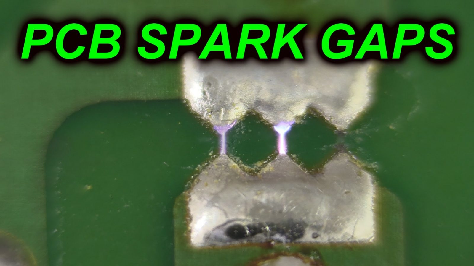
In this tutorial Dave explains what a PCB spark gap is and how it can be a useful zero cost addition to your PCB layout to help prevent ESD damage.

EEVblog #678 – What is a PCB Spark Gap
He shows how to easily design them into your board and calculate the approximate voltage rating.
And of course has some fun applying 5kV to some gaps to show how them at work.


For more detail: EEVblog #678 – What is a PCB Spark Gap?


About The Author

Ibrar Ayyub

I am an experienced technical writer holding a Master's degree in computer science from BZU Multan, Pakistan University. With a background spanning various industries, particularly in home automation and engineering, I have honed my skills in crafting clear and concise content. Proficient in leveraging infographics and diagrams, I strive to simplify complex concepts for readers. My strength lies in thorough research and presenting information in a structured and logical format.

Follow Us:
LinkedinTwitter

Leave a Comment

Your email address will not be published. Required fields are marked *

Scroll to Top