In this lab you will be using a program to enter a schematic and lay out a printed circuit board (PCB) that will then be manufactured. At this point of the semester you don’t know enough to design your own circuit, so I am giving you one that we will use again later in the semester. The program that we will be using to do the schematic entry is called Multisim and the program for the PCB layout is called Ultiboard This lab will serve as an introduction to schematic entry and PCB layout.
The Lab
Schematic Entry
Starting out
Step 1. The software for this lab should be on any of the PC’s in room 310 or 212 of Hicks. Log on to one of the computers and start the program called “MultiSim” (it is in the “National Instruments/Circuit Design Suite 12.0” program group). The schematic defines all the interconnections between various circuit elements.
First, we’ll add a title block to identify the schematic as your own. Now download the file SwatTitleBlock.tb7 and then from the MultiSim menu choose Place→Title Block and choose that file. Place the title block onto your schematic. After placing it, you can right-click on the title block to move it exactly into place (e.g., the lower right corner). Now double click on the title block and change the data in the block to reflect your circuit.
Save your circuit — You should save your circuit someplace you can access it later (i.e., swatfiles, or google drive…). Files stored on the local PC may be deleted. Also, having the files stored remotely allows you to work on your design from any of the PC’s running Multisim. Make sure that the filename is unique — some permutation of the names of the people in the group is good. You will be emailing me your design later on, and a unique name will help me keep your design from being confused with another.
Picking Components for the Schematic
Step 2. At this point we want to pick the components that will be in your design (a circuit that flashes LED’s) and put them on the schematic diagram. Go to Place→Component and select the “Corporate” database, then select the “Basic” group, the “LED” family and finally select the “LED-R” as the component by hitting the “OK” button.. If you can’t find one of the parts, hit the “Search…” button on the right side of the dialog box; this should make the missing parts appear.
Place the component anywhere on the diagram. This component is an LED (Light Emitting Diode).
The rest of the components are listed in the table below. They are all in the Corporate database. Note that some components are used more than once, so you need to place multiple copies.
| Quantity | Group | Family | Component | Description. |
| 1 | Basic | LED | LED-G | This LED will be used as an indicator that power is applied. |
| 1 | Basic | LED | LED-R | This LED is controlled by a PMOS transistor. |
| 4 | Basic | LED | S-WhiteLED_LCW6SG | 4 LED’s controlled by an NMOS transistor. |
| 3 | Basic | Resistor | 680Ohm | Used to limit the current through the LED’s and set frequency of oscillation. |
| 1 | Basic | Resistor | 2kOhm | Sets frequency of oscillation. |
| 2 | Basic | Resistor | 120Ohm | Limits current in white LED’s |
| 1 | Basic | Resistor | Potentiometer | Adjusts frequency of oscillation. |
| 2 | Basic | Capacitor | 0.01uF | Used by timer IC (555) that makes LED’s blink. |
| 1 | Basic | Capacitor | 100uF | |
| 1 | Analog | FUN | S-555_SOIC | The Integrated circuit that blinks the lights. |
| 3 | Misc | Connector | S-HDR1x2 | Allows dis/connection between two points |
| 1 | Misc | Connector | S-TestPnt | A test point that will be useful for debugging. |
| 1 | Sources | Battery | Battery_9V | A 9 volt battery. |
| 1 | Transistors | NMOS | S-IRFD024 | NMOS Transistor (note arrow points inward, towards transistor) |
| 1 | Transistors | Transistors | S-IRFD9024 | PMOS Transistor (note arrow point outward, away from transistor) |
| 1 | Electro_Mechanical | SSwitch | S-Hole125 | Mounting hole for board. |
Next you need to place some components from the MultiSim database. Go to Place→Component and choose
- Database: Multisim Master
- Group: Sources
- Family: POWER_SOURCES
- Component: Vcc
Place two or three Vcc symbols on your schematic. Also place two or three GROUND symbols symbols from the same Database, Group and Family. As you are doing your design use as many or as few of these power symbols as you need to make a neat drawing.
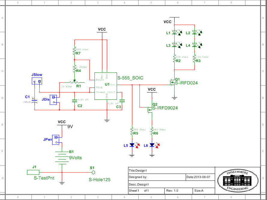
Your schematic should now look something like the circuit shown below. Your part numbers may be different, and I have renamed some of the components (Select component, Right-Click, then Properties→Label→RefDes); you should do the same. I also changed the default voltage of Vcc to 9 V (Properties→Valuel→Voltage (V))
Step 3. Now you need to make all the connections. Lets start with some simple ones.
First we will connect the battery. The jumper labeled “JPwr” is used as on/off switch (if jumper is across pins, the battery is connect to Vcc, else it is not). We also connect the test point and the mounting hole to ground.
Complete the rest of the connections as shown in the diagram below. Your diagram may look substantially different than mine, depending on the placement of your parts. Neatness counts — make your diagram as neat as possible. Note, wires that cross but don’t have an intersection symbol (a dot, as shown above) are not touching. If you need to add a junction to make a connection you can go to Place→Junction. (pdf version of circuit)
Important: Double check all your connections. Have one member of your group read off connections from my diagram while another checks it against your own diagram. This sound tedious, but takes little time. Any connections that get fabricated incorrectly are much more difficult to change later on.
Select a trace that is connected to Vcc, right click on it and choose Properties→PCBSettings→Trace widths→Default and set it to 20 mils. Repeat for ground and the the wire between JPwr and the 9 volt battery. This will set the trace widths for the power lines on the printed circuit board to be somewhat broader than the signal lines.
Save your schematic.
PCB Layout
Step 4. From Multisim, save your schematic. Now go to Transfer→Transfer to Ultiboard 12.0. Save the files that are created in the same directory you saved your schematic. Hit “OK” on the “Import Netlist” window. Your window should look something like the one below:
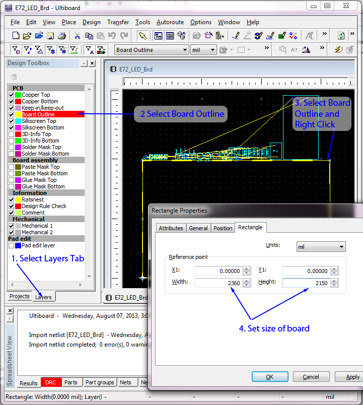
Step 5. The objects at the top of the screen are the components that form your circuit, the large yellow rectangle is the circuit board. The circuit board is large than we want. To make it smaller, select the “Layers” tab in the lower left corner and select “Board Outline”. Now use the cursor to select the yellow rectangle, then right-click and choose “Properties”. Change the width to 2360 mils (thousandths of an inch) and the height to 2150 mils to define a board that is 2.36×2.15 inches. (Note: you must use exactly 2.36×2.15 because all boards must be the same size because they are fabricated in a rectangular array.)
For more detail: Schematic Entry and PCB layout