Contributed by Publitek European Editors
10/15/2013
Power MOSFETs have become very popular in power electronics designs because of their low capacitance and good high-frequency switching characteristics. They have reached into many applications and are helping to open up new markets in applications, from hybrid and electric vehicles through solar power to extreme-environment exploration. The unifying factor of these environments is heat. Automotive engines and solar panels can generate heat that pushes junction temperatures in power devices far higher than 100°C. Such heat can badly affect power semiconductors that are not designed to cope.
Power semiconductors all have temperature limitations. Leakage current increases with temperature and this can accelerate effects that lead to breakdown conditions that can damage circuitry and cause other hazards.
All semiconductors are rated for a given maximum reverse voltage. If the device is operated above this voltage, high electric fields will be generated in reverse-biased electric fields. These electric fields are strong enough to accelerate free-charged particles to high energies. When these accelerated carriers strike electrons bound to atoms, they transfer enough energy to break their atomic bonds and form electron-hole pairs. Under the high electric field, they will be accelerated in opposite directions and can, potentially, strike other fixed electrons, breaking them free in turn. The result is avalanche breakdown, which can destroy the diode layers within power semiconductors, rendering the devices non-functional.
Even if the device is not irreparably damaged, as some devices are designed to withstand a certain amount of avalanche current, a hysteresis effect means the voltage has to drop significantly before the reverse current is shut off, potentially causing damage to other components in the system.
In silicon, heat tends to accelerate the process of avalanche breakdown because higher temperatures will impart thermal energy to valence electrons in the crystal lattice of the power device. As more thermal energy is absorbed, some of those valence electrons will break free of their bonds and move into the conduction bands. Inductive loads increase the risk of breakdown because of the high reverse-bias conditions they can impose on the diode junctions inside a power transistor when used with switching power-supply circuitry.
One answer is to move to wide-bandgap materials such as silicon carbide or gallium nitride as the probability of electrons being promoted to the conduction band by thermal energy is lower than with silicon. However, not many suppliers make these devices, particularly transistors. Another approach is to fabricate more rugged silicon devices that prevent subtle weaknesses in design causing failures too easily.
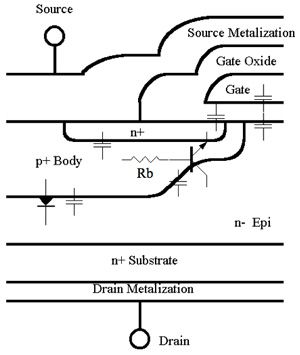
The most common failure mode is the activation of a parasitic bipolar transistor between the source and drain that can form when the electric field is high at the point where the junction under the gate bends most tightly. This effect is most prominent at high temperature because the resistivity of the silicon increases. As the resistance increases, the voltage drop under constant current rises in turn. If that voltage drop reaches the point where the parasitic transistor turns on, it is likely to remain switched on with damaging results.
Typical power MOSFETs are made using vertical processes such that the transistor channels run through the body of the die from bottom to top. This allows multiple sub-transistors to be arrayed across the surface of the die, often in a hexagonal pattern to maximize packing density. Such devices exhibit lower on-resistance values thanks to the use of many parallel channels
For more detail: MOSFETs that Can Take the Heat