January 9, 2013 (1 hour):
Met as a team after class to discuss preliminary project proposal.
January 10, 2013 (2 hours):
Met as a team after class to finish writing preliminary project proposal.
WEEK 01 SUMMARY
Accomplishments: Submitted preliminary project proposal.
Weekly Work Total: 3 hours
Project Work Total: 3 hours
Week 02
January 16, 2013 (2 hours):
Met as a team to write final project proposal and develop PSSCs for presentation. Started developing a parts list to generate a rough project budget.
We came up with the following block diagram and split up the workload based on the main functional units(SMS module, server-side, power, strobe lights).
WEEK 02 SUMMARY
Accomplishments: PSSC and project proposal finalized.
Weekly Work Total: 5 hours
Project Work Total: 8 hours
Week 03
January 23, 2013 (2 hours):
Worked as a team to finalize the PSSC’s based on feedback from course staff and peers. Decided to implement the DMX512 protocol to control strobe lights. Also decided to add an SD card slot to allow users to upload files with preferences:
-Blacklist and white list for songs
-WIFI settings
-Lighting preferences
-Sound effect files
Original plan was to add a camera, to increase hardware on device, but the camera just did not fit with the goal of the project. The SD card is much more practical.
January 24, 2013 (2 hours):
Completed homework 2.
WEEK 03 SUMMARY
Accomplishments: Homework 2 and updated PSSCs. Finalized major functionality
Weekly Work Total: 4 hours
Project Work Total: 12 hours
Week 04
January 29, 2013 (5 hours):
Worked on constraint analysis and started looking at parts for our major pieces of functionality. Found GSM Module and investigated DMX512 protocol and implementation. Looked, but could not find a DMX512 reference in Potter.
GSM Module requires UART and an separate SD card slot. Basic operations for sending and receiving SMS messages is fairly simple. Should investigate more complex features like the ability to buffer messages. We are not expecting an overload of text messages, but with lights requiring more timely processing, it is probably better to hold received texts until that can be parsed. Here are some good references:
– This site talks about Arduino, but is a still a good reference.
– This site lists commands that can be sent over UART.
Also looked into details of DMX512 protocol. Decided we could send DMX control signals using UART, with a voltage regulator. Some important details about the DMX512 protocol:
– Uses RS-485 standard to define electrical properties
– Must send a signal every second
– Lights are daisy chained, so one DMX port on our device could theoretically control 512 lights (hence the 512 in DMX512)
– Lights are addressed sequentially, and packets are sent to consecutive addresses.
– Need to find a way access the actual protocol document which is for sale for $50.
February 1, 2013 (1 hour):
Met with group from management class to discuss how collaboration for their business plan. They brought a different perspective looking at the project from a marketing stand point. There were clearly some points were the requirements for our projects were not entirely compatible. Overall collaboration seems like it could add to both of our projects.
WEEK 04 SUMMARY
Accomplishments: Completed constraint analysis and part list. Met with management team
Weekly Work Total: 6 hours
Project Work Total: 18 hours
Week 05
February 6, 2013 (2 hours):
Ordered major components after class:
– 6 sample microcontrollers from Atmel
– Raspberry Pi
– GSM Module and board connector
– SIM Card slot
– SD Card Slot
– DMX converter and female connector
– LCD display
More detailed parts may need to be order later. Did not order analog components or LEDs for the box.
Set up our lab station and logged into the computer.
WEEK 05 SUMMARY
Accomplishments: Ordered parts. Packaging design
Weekly Work Total: 2 hours
Project Work Total: 20 hours
Week 06
February 11, 2013 (1 hours):
Downloaded EAGLE on personal computer to practice with. Walked through Sparkfun PCB schematic and tracing tutorials.
February 12, 2013 (2 hours):
Ordered more parts including voltage regulator for the power supply. Looked into hardware associated with GSM module and started drawing up a schematic.
Also found some good resources:
– Breakout board schematic
– GSM Module Hardware Spec
– GSM User Manual
Also found better SIM slots:
SIM4050
SIM4055
February 13, 2013 (3 hours):
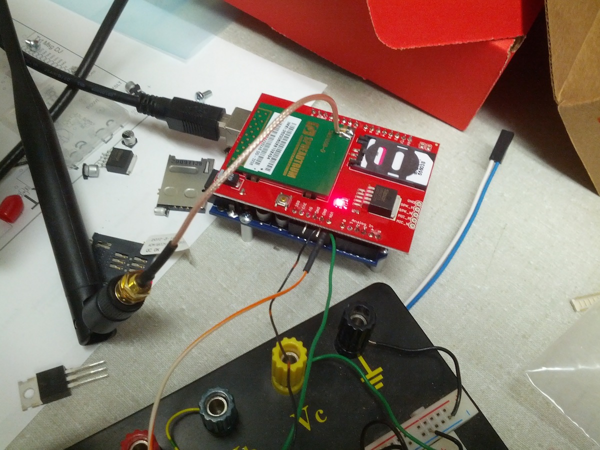
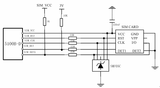
Worked on schematic for the GSM Module. Researched circuits involved in GSM module and SIM card reader. Need to order a SIM card reader and electrostatic discharge IC still. SIM card reader requires a good deal of protection from ESD. Created the following circuit from the GSM Module hardware guide in Eagle:
Still need to make SIM card slot in EAGLE.
February 13,2013 (6.5 hours):
WEEK 06 SUMMARY
Accomplishments: Ordered parts. Packaging design. Completed some custom footprints and circuits in EAGLE
Weekly Work Total: 12.5 hours
Project Work Total: 32.5 hours
Week 07
February 18, 2013 (5 hours):
Worked on preliminary layout of parts including rough parts positioning and overall size of board. Made some changes to the schematic. Some of the considerations for the parts layouts are: – Slots (SD, SIM) need to be in the back of the device for easy access.
– Most DMX circuitry needs to be in the back of the device to avoid long connections between DMX female connector and DMX driver.
– GSM module should be as isolated as possible. It uses an unusual power supply and has high and quickly varying current requirements which could generate significant noise. Additionally, the module itself will be the be receiving and transmitting RF signals which could generate more noise despite shielding.
– GSM module needs to be on edge of the board so antenna can attach to side of the device.
The image below shows the current state of the layout without any traces.
February 19, 2013 (6 hours):
Prepared for TCSP on preliminary PCB layout. Moved headers for debugging microcontroller to the area surrounding the microcontroller. This will allow for easier access when debugging and if any modifications or additional features need to be added after the PCB has been manufactured. Moved all individual components including resistors and transistors into locations that will make routing as easy as possible. I have started considering routes for power and ground, but most of the tracing has not been done. Considerations for the traces are as follows:
– Circuits with different voltage requirements should be separate.
– Power supplies should be as close as possible to final destination to reduce noise
– Traces for the power source for the GSM module should be around 50 mils because of potential 2A draw. This number is certainly on the safe side, but it without prior experience with PCB design this is the best approach.
– All other power supply traces should be thick but not necessarily as thick as GSM module traces. Other power supply traces will be about 30 mils.
– Large ground and power planes will be used to reduce source and ground immpedances.
Another note related to power supplies is the need for heat sinks. The only voltage regulator that could potentially use a heat sink is the 3.8V regulator for the GSM module which could at times provide as much as 2A. If the supply was a constant 2A, a heat sink would be necessary, but because the 2A spikes are very intermittent, it will not be necessary.
Here is an image of the current state of the layout and traces. Not all traces are complete, but power and ground are in place.
February 21, 2013 (6 hours):
Modified PCB layout from TCSP feedback and competed all traces. Moved decoupling capacitors for the micro to the bottom side of the board. The PCB is still in a preliminary stage, so it needs to be double checked for functionality and acute angles. All electrical connections have been made and all footprints match. Design was completed with previously stated considerations in mind. Below are some images of the final layout.
For more detail: John Doherty’s Lab Notebook