If you previously worked(or currently working) with small 8-bit microcontrollers, like ATTiny or PIC12, you’ve probably encountered a fundamental problem of not having enough GPIO pins for your needs or project requirements.
Upgrading to a larger MCU is only one of the options, but as usual there is an alternative. In this article I will explain how to use shift registers in some common situations in order to expand the I/O capacity of your microcontroller. As an example I will use an ATTiny13A and a 74HC595 shift register.
Step 1: First date
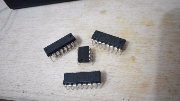
Shift register is a semiconductor device which accepts serial input and produces parallel or serial output depending on how you use it. Also, as almost all semiconductor ICs, shift registers have gotten very cheap, so instead of spending relatively small sum of +$1.00 on a single different microcontroller you should get a handful of those 74HC595’s at $0.12 apiece.
74HC595 is an 8-bit serial-in, serial or parallel-out shift register with output latch and 3-state output. In order to understand what it is let’s look at the functional diagram of this device:
We feed serial input bit-by-bit through DS pin, while providing clock signal to SHCP pin in order for shift register to shift its contents. If we want to save the 8-bit input data, we have to toggle STCP pin to latch the contents onto the storage register. This gives us the ability to “hold” the old output while feeding 8 bits of the next output. Pin Q7S is used for cascading, which means if we have 2 shift registers and we connect Q7S output of the first one to the DS pin of the second one, we get a 16-bit shift register! And, as you should’ve noticed, we only need 3 pins to use its essential functions (DS, SHCP and STCP).
 A pinout diagram for our shift register is shown above.
Most of the pins were described earlier, but there are 2 more left:
- OE (Output Enable): is active low. When set to 1 it disables the output and sets pins Q0…Q7 to a high-impedance state.
- MR(Master Reset): is also active low. When set to 1 it clears the contents of the shift register (not the latch).
We are not using either of these pins for this project, so OE must be connected to ground, while MR is connected to VCC, which will keep output pins in the on-state all the time and will prevent shift register from resetting. In order to clear the contents of the shift register we are just going to send it the value 0x00 just like regular data. To learn more about this device please read the 74HC595 datasheet.
Step 2: Example #1 [OUTPUT]
Code
We are going to read an 8-bit value from ADC3 (most significant bits) and then pass the corresponding output value to our shift register.
To be more specific I’ve made a table of values for I/O states:
| ADC3 value | Output value | Segments on |
|---|---|---|
| 0..40 | 0xFF | 0 |
| 41..80 | 0xFE | 1 |
| 81..120 | 0xFC | 2 |
| 121..160 | 0xF8 | 3 |
| 161..200 | 0xF0 | 4 |
| 201..255 | 0xE0 | 5 |
NOTE: Because it is a common anode LED indicator we need to set the appropriate pin LOW whenever we want it to light up.
Now, let’s write some code.
In short, we need to set up a Timer Overflow interrupt, which will read the current state of ADC3 and send the corresponding value to our shift register approximately every ~27ms.
SEND_BYTE subroutine sends an 8-bit stream of data and latches it in the shift register. This is a bit simplified function, but with some minor improvements can be used universally.
I wrote most numbers in binary form, so it will be easier (at least for me) to see which LEDs are enabled and which flags are set.
Step 3: Example #1: Code
The code is written in AVR Assembly. If you work with controllers like ATTiny – it is a must! It looks scary, but in reality it’s much simpler and easier than C.
Another reason for using assembly language is that this code only needs 148 bytes of space after compilation, while Arduino IDE produces 644 bytes of binary output for the same code (haven’t tested in AVR GCC), so if you want to expand functionality of your Tiny project, you have less than 400 bytes left to work with…
/*
 *	Shift register demo #1
 *
 *	ATTiny13A Running @9.6MHz
 *	ADC running @150kHz
 *
 *	PIN ASSIGNMENT:
 *		PB0 - Shift Register Clock
 *		PB1 - Shift Register Serial Data
 *		PB2 - Shift Register Latch(Store)
 *		PB3 - ADC3 (Potentiometer input)
 *		PB4 - [NOT USED]
 *		PB5 - RESET
 */
.include "tn13Adef.inc"
.def	A = R16	; g.p. variable and/or function argument
.def	B = R17	; Used in SEND_BYTE and ADC_START as temporary storage
.def	LED = R18	; stores current LED output
.def	BCT = R19	; Bit counter for SEND_BYTE
.equ	SRCK = 0	; PB0 = Clock
.equ	SRDA = 1	; PB1 = Serial Data
.equ	SRLC = 2	; PB2 = Latch

/*	INTERRUPT VECTORS	*/
.org	0x0000
rjmp	RESET		; Reset interrupt
.org	0x0003
rjmp	TC0_OV		; Timer1 interrupt

/*
 *	START!!!
 */
RESET:
        /*	SETUP STACK	*/
	ldi	A, low(RAMEND)	; Set stack pointer
	out	SPL, A
	/*	SETUP PINS	*/
	ldi	A,0b0000_0111	; Set output pins PB0..PB2
	out	DDRB,A
	/*	SETUP TIMER1	*/
	ldi	A,0b0000_0101   ; Set Timer Prescaler (1024)
	out	TCCR0B,A	; This will cause Timer Interrupt every ~27ms
	ldi	A,0b00000010	; Enable Timer0 Overflow Interrupt
	out	TIMSK0,A
	/*	SETUP ADC3	*/
	ldi	A,0
	out	ADCSRB,A	; Disable autotrigger(Free running)
	ldi	A,0b00001000	; Disable Digital Input on PB3(ADC3)
	out	DIDR0,A
	ldi	A,0b00000011
	out	ADMUX,A		; Source:ADC3, Align:RIGHT, Reference:VCC.
	ldi	A,0b10000110
	out	ADCSRA,A	; Enable ADC with prescale 1/64
	/*	RESET REGISTERS	*/
	ldi	A,0x00		; clear A
	ldi	LED,0xFF	; Set all LED's to OFF(1-off, 0-on)
	rcall	SEND_BYTE	; Clear display
	sei			; Enable interrupts

/*	Main loop	*/
MAIN:
	rjmp	MAIN

/*
 *	Sends 8-bit data from LED register to Shift Register
 */
SEND_BYTE:
	ldi	BCT,0b1000_0000	; Set Bit counter
next_bit:
	mov	B,LED		; Move data byte to temp
	and	B,BCT		; Check bit
	breq	zero		; Set Data to 0
	sbi	PortB,SRDA	; Set Data to 1
	rjmp	shift		; shift
zero:
	cbi	PortB,SRDA
shift:
	sbi	PortB,SRCK	; CLK up
	nop
	cbi	PortB,SRCK	; CLK down
	clc			; Clear Carry flag
	ror	BCT		; Shift bit counter
	brne	next_bit	; Next iteration
	sbi	PortB,SRLC	; When done, Latch
	nop
	cbi	PortB,SRLC
	ret			; Done
/*	Start ADC conversion. Saves result to A	*/
ADC_START:
        sbi	ADCSRA,ADSC	; Start ADC conversion
adc_wait:
	sbic	ADCSRA,ADSC	; Check conversion status
	rjmp	adc_wait	; Skip jump if completed
	in	A,ADCL		; Get low bits
	in	B,ADCH		; Get high bits
	lsr     B		; Shift 2 bits to the right
	ror A			; through Carry
	lsr B
	ror A
	ret
/*	Timer 0 overflow interrupt	*/
TC0_OV:
	rcall	ADC_START	; start ADC0 Conversion
	/* Compare Input, Set output */
	cpi	A,0xC8		; A>=200?
	brlo	gt_160
	ldi	LED,0b11100000
	rjmp	sr_write
gt_160:				; A>=160?
	cpi	A,0xA0
	brlo	gt_120
	ldi	LED,0b11110000
	rjmp	sr_write
gt_120:				; A>=120?
	cpi	A,0x78
	brlo	gt_80
	ldi	LED,0b11111000
	rjmp	sr_write
gt_80:				; A>=80?
	cpi	A,0x50
	brlo	gt_40
	ldi	LED,0b11111100
	rjmp	sr_write
gt_40:				; A>=40?
	cpi	A,0x28
	brlo	lt_40
	ldi	LED,0b11111110
	rjmp	sr_write
lt_40:				; A<40
	ldi	LED,0b11111111
sr_write:
	rcall	SEND_BYTE	; Send byte to shift reg.
	reti			; return
For more detail: Getting more I/O pins on ATTiny with Shift Registers